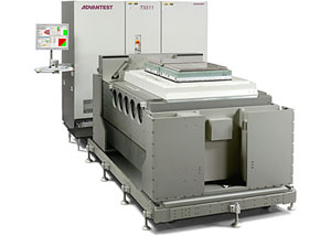
Industry-best 8Gbps test speed and timing accuracy of ±40ps
With a maximum test speed of 8Gbps, the T5511 is the world's fastest memory testers, supporting the very fastest GDDR5-SDRAM devices with capacity to spare. Furthermore, since all the system's test pins support 8Gbps, no reduction in parallelism occurs when operating at high speed.
Built-in clock training control functionality
Essential for new DDR4-SDRAM and GDDR5-SDRAM device test, clock training functionality is built into the T5511's hardware. This allows throughput improvements impossible when relying on software for this function.
Simpler test program creation
The T5511 also features a hardware CRC code generator function, necessary for cutting-edge DDR4-SDRAM and GDDR5-SDRAM device test. The dedicated hardware generates CRC codes automatically, reducing the burden on the operator and making it simpler to create test programs. Additionally, the T5511 runs Advantest's "Future Suite" tester OS, allowing operators to utilize the extensive library of program data created for T55xx series test systems.
"Lab to fab" flexibility
System configurations range from 384 pins for R&D use through to a maximum of 6,144 pins for volume production. The T5511's "lab to fab" flexible configurability allows customers to hold capital investment to a minimum, while achieving maximum test efficiency.
Diverse DRAMs, One Test Solution
Dynamic random access memory (DRAM) is the most commonly used type of commodity memory device for personal computers and workstations. It is also widely employed in servers and clients, and used extensively in graphics and mobile applications. Though ubiquitous, the pace of DRAM technology changes and advances quite quickly; there is a high degree of variation – in speed and function – between the application classes. The ultra-fast GDDR5-SDRAM chips used for graphics need functions such as clock training and CRC (cyclic redundancy check) to ensure their reliability and high-speed performance. Meanwhile, DDR4-SDRAM for servers and clients will soon achieve twice the bandwidth of mainstream DDR3-SDRAM and functionality equal to GDDR5. In the mobile and graphics segments, bus widths of x32 and x64 are now mainstream, and Wide I/O DRAMs with a 256-bit wide interface are expected to be standardized in the near future.
The diverse requirement from the final application, the development in DRAM technology requires optimal test solutions that can support each new device generation and application, while cost-control imperatives demand a single-platform solution supporting various types of DRAM, which can be flexibly deployed from R&D through to volume production.
| Target Devices | DDR4-SDRAM, GDDR5-SDRAM |
|---|---|
| Parallel test capacity | 256 (×8 I/O) |
| Maximum test speed | 4GHz / 8Gbps |


