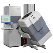
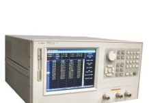
Enabling Versatility, Scalability, Massive Parallelism and Breakthrough Cost-of-Test for FLASH, DRAM & MCPs
Advantest redefines the industry with the revolutionary V6000. Through its patent-pending Active Matrix™ and sixth-generation Tester-Per-Site® architecture, the V6000 delivers breakthrough cost-of-test, parallelism and yield for engineering, wafer sort and final test of both Flash and DRAM. The versatility of the V6000 allows testing of Flash and DRAM on the same test solution. The V6000 is scalable over time to greatly extend the useful life of your capital investment.
V6000 Platform
With the new V93000 Smart Scale Generation, the engineers at Advantest are addressing the challenges of high integration CMOS technology:
The V6000 is the complete test solution for all memory test needs – Flash, DRAM and MCP – and from engineering development to high-volume production and for both wafer sort and final test. With its scalable platform architecture and optimized tester resources to efficiently and economically test all memory types, the V6000 solves the widest variety of memory test issues.
The sixth generation Tester-Per-Site® architecture makes memory testing much more efficient – the multi-site controller and multi-APG are dynamically configurable to match specific applications and device types. With a consistent platform architecture providing complete test transportability and stability, you gain new levels of efficiency in migrating tests from design to sort to final test.
The V6000 addresses today’s need for highly flexible and configurable systems to test the full spectrum of memory devices at the lowest possible cost. In addition, because of its unique scalable platform architecture, the V6000 has unequaled versatility and capability to meet tomorrow’s increasingly complex, rapidly expanding memory test requirements – protecting your investment by providing upgradability well into the future as opposed to the need to add new test platforms.
All the V6000 testers also share the same operating system software, hardware and interface, allowing users to develop, share and move test programs between testers as devices go from engineering and characterization to wafer sort and final test. With minor modifications, test programs from Advantest’s popular V5000 family of testers can be used with the V6000 platform. The V6000 is water-cooled, requiring a smaller footprint and using less energy than air-cooled systems.
SmartRA

SmartRA for the V6000 WS
Scalable, flexible and cost-effective RA solution for DRAM at wafer sort
SmartRA, an option for the V6000 WS, provides the performance needed to conduct redundancy analysis on DRAM devices, thereby allowing manufacturers to achieve their throughput and yield goals for wafer sort.
SmartRA provides flexible performance for a wide variety of cases that a manufacturer might encounter, including low or high test frequencies, and low or high levels of complexity with redundancy design. SmartRA eliminates the possibility of timeouts (during which RA time exceeds the shorter pattern time made possible by the V6000's parallelism), thereby maintaining high throughput and yields. SmartRA's open architecture makes it possible to use either Advantest RA algorithms or algorithms that customers have defined themselves; customers need not be tied to proprietary software architectures. The open architecture also uses off-the-shelf high-performance blade servers, enabling customers to add only the performance required for their immediate needs, without impacting the test cell footprint, and do so at minimal cost. The testing solution will remain viable and cost-effective into the future.
Ample and scalable performance for wide range of test cases
A solution for all cases that a manufacturer might encounter, SmartRA handles low or high test frequencies, and low or high levels of complexity with redundancy design.
Here's why greater performance is so important, specifically with RA of DRAM. The V6000 WS makes it possible to double test frequency, which reduces functional test time. Consequently, RA times can be longer than the pattern time-i.e. no longer hidden, but rather exposed-creating the possibility of timeouts, which drag down yields. As test requirements evolve, SmartRA ensures that RA can remain hidden. SmartRA, with its higher performance, reduces the RA time to once again hide within the pattern time, eliminating timeouts between patterns. High throughput and yields are maintained.
Flexibility of an open architecture
SmartRA's design is based on an open architecture. In contrast to proprietary software architectures from other companies, manufacturers can use RA algorithms they define themselves, or use Advantest turnkey RA algorithms. Additionally, by being based upon the long-tester-life V6000 platform, as well as off-the-shelf blade servers, the testing solution will not become obsolete when today's devices do. Manufacturers only pay for what's needed now, while remaining ready to adapt to future needs, all on the same platform.
Cost-effective immediately and as needs change
performance blade servers, which are separate from, yet highly integrated with, the core test solution, the V6000 WS. As a result, when more performance is needed, processing power can easily be added, virtually without limits, and without impacting the test cell footprint. With support of up to eight V6000 WS test cells with a single server rack, manufacturers always have the right performance at the lowest cost.
Testers from other companies include the RA processing within the tester architecture. In order to maintain throughput and yields on such systems, customers need to spend considerably more on processing power.
Features & Benefits
| Feature | Benefit |
|---|---|
| High RA performance | Delivers enough processing power to keep RA time hidden behind the shorter pattern times of the V6000's scalable parallelism |
| Scalable servers | Matches V6000 hardware platform scalability, including RA support for 1 TD test capability for DRAM wafer sort for each functional test. Scale number of servers without increasing test footprint |
| Open software architecture | Enables use of customized RA software algorithms or those provided by Verigy |
| Turnkey solution | Speeds time-to-market |
| Scan Controller per test site | Accelerates scan, compression, preprocessing, and transfer of fail data for RA and bitmapping |
| Enhanced LANComm | Accelerates data transfer to the RA server farm for analysis and bitmapping |
Active Matrix

Active Matrix Fully Integrated into Tester
Revolutionary technology enables 4x performance, increased throughput and yield through massive parallelism and significantly improved signal fidelity
With the V6000 test solutions, Advantest introduces Active Matrix?, the innovative patent-pending technology that enables increased throughput through increased parallelism, and increased yield through significantly improved signal fidelity.
Thanks to Active Matrix, the V6000 can deliver the breakthrough cost-of-test, scalability and flexibility you need to enable long functional life for both Flash and DRAM testing. Increased performance equals higher speeds and increased signal fidelity, resulting in reduced test time and higher yields. Fully integrated into the tester, Active Matrix delivers:
- 18k I/O pins
- 4k programmable power supplies
- Minimum cable length connecting to pin electronics
The Active Matrix provides what no other test solution on the market can:
Four times the number of pins = four times the parallelism at half the cost per pin
- Pin electronics are moved to the interface layer, located in a cost-optimized pin electronics ASIC to achieve up to 18K pins per system
- Custom ASICs, with drivers and comparators, produce four times the parallelism of traditional test solutions, at significantly lower costs (50 percent less per pin)
- Matches or exceeds the parallelism of other testers, without the signal degradation caused by sharing pins or the yield loss caused by shorted pins on a shared channel
75 percent reduction in distance between the pin electronics and probe card improves signal fidelity and yield
- Active Matrix ASIC enables close proximity to the probe card to provide optimal signal performance and parallel reads
- Reduced capacitive load-to-drive helps to eliminate excessive guard banding caused by long tester transmission lines that don't match real-world device environments
Tester-Per-Site® Architecture
6th Generation Tester-Per-Site® Architecture Enables Scalability, Versatility, Industry-Highest Parallelism and Industry-Lowest Cost-of-Test for FLASH, DRAM & MCPs
Advantest's Tester-Per-Site architecture utilizes a multi-site controller and multiple APGs that are dynamically configurable to match specific applications and device types. With each successive generation, our Tester-per-Site architecture has increased parallelism, improved performance, and lowered cost-of-test.
Our sixth generation Tester-Per-Site architecture underpins the new V6000 Series with Active Matrix, enabling optimized test of all memory device types (NOR, NAND, DRAM, SRAM, and MCP) for engineering, wafer sort and final test – at the much lower cost of a Flash tester. The architecture coupled with the Active Matrix supports up to 18K I/O pins, scalable power supplies and scalable performance up to 280 MHz/880 Mbps.
A Long History of Tester-Per-Site Architecture Innovations
The first generation Tester-Per-Site architecture debuted in 1996 on the V1300 test system and delivered an innovative feature set – individual test site controller, algorithmic pattern generator (APG), error catch ram (ECR), pin electronics, and programmable power supplies (PPS) – as well as new performance capabilities, including per-site scalability, I/O flexibility and adaptive test, enabling optimized test times resulting in lower cost-of-test.
The V3300, using second generation architecture, doubled the number of pin resources from 512 to 1024 I/O and test speed from 10 to 20 MHz. With each successive generation of the architecture, features and performance have continued to grow.
In 1999, the V4400 offered our third generation Tester-Per-Site architecture, fully integrated and with new system features including water cooling and test head electronics, further increasing performance to 2304 I/O pins and 50 MHz – 100 MHz in mux mode, and enabling high parallelism for all memory devices. The third generation architecture further enabled the easy transfer of test programs developed on low-cost engineering systems onto volume production systems.
The fourth generation of the architecture, launched with the V5000 series in 2003, delivered dynamically configurable multi-site controllers and scalable APGs, doubled available resources and improved performance – to 4608 I/O pins and 100 MHz.
The fifth generation Tester-Per-Site architecture of the V5500, combined with the Programmable Interface Matrix, optimized single-insertion testing of MCPs with multiple memory types (including Flash, DRAM and SRAM) and high parallelism Flash testing. This resulted in industry-leading tester utilization, throughput and lowest cost-of-test. Available pin resources grew more than five times over the previous generation to 24,576 I/O pins.


Comments are closed.